Types of power supplies
All power sources can be divided into two large classes:
- pulse;
- transformer
These terms are not very precise - a transformer power supply can have both a linear and a switching voltage stabilizer, and a switching power supply contains a transformer.
Each type has its own advantages and disadvantages based on the principle of operation. A transformer power supply with a linear voltage regulator distributes energy between the load and the regulating element (usually a power transistor) and is a voltage divider. One arm is the control element, the other is the load.
We recommend: Types of power supplies and their purpose
When the voltage across the load decreases (for example, due to an increase in current consumption), the transistor opens slightly and maintains this voltage constant. When the voltage across the load increases, the process is reversed - the transistor closes. This is how the stabilization process occurs.
Operating principle of a linear stabilizer.
Disadvantages of this scheme:
- it is required that the input voltage be noticeably higher than the output voltage;
- a current equal to the load current constantly flows through the regulating transistor - a lot of power is wasted;
- The efficiency, even theoretically, cannot exceed the ratio Uout/Uin.
The advantages are:
- relatively simple and inexpensive scheme;
- the output voltage is free from high-frequency parasitic components (power supply interference is minimal).
A switching power supply operates on a different principle. Here the energy is distributed over time. Key transistors have only two states - they are either completely open or completely closed. The duration of the open position determines the average current through the primary winding of the transformer and the average voltage on the output capacitors of the filter (and, accordingly, on the load). It is convenient to control this process using the pulse width modulation (PWM) method, when the conversion frequency remains constant and only the pulse length changes.
In an ideal pulsed source of stabilized voltage, the switches in the open position have zero resistance, there is no voltage drop, and in the closed position there is no current at all. Therefore, energy is not dissipated in transistors. In practice, not everything is so rosy. There are no ideal transistors, so in the open state a certain voltage drops across them (resistance is not zero), and in the closed state there is a leakage current (resistance is not infinity).
But the main losses that reduce efficiency occur for another reason. Transistor switches do not switch from one state to the opposite instantly. This takes time, depending on the speed of the element. During the transition, a through current flows through the transistor, the voltage across it drops - therefore, power is released. These losses are called switching losses, their magnitude depends on the conversion frequency.
Real and ideal switch in switching power supply.
But still, the efficiency of such a source is higher than that of a linear one. And this is the main advantage of such a scheme. Another advantage is the smaller size and weight of the power source. This is achieved due to the fact that the conversion is carried out at a fairly high frequency - up to several tens of kilohertz. Therefore, the heaviest and most bulky element (power transformer) turns out to be light and compact. The main disadvantage is the complexity of the scheme.
Typically, linear voltage sources are used for currents up to 2 A. Closer to currents of 3 A and higher, the advantages of pulse generators begin to outweigh.
Main components of a regulated power supply
The transformer power supply in most cases is made according to the following block diagram.
Transformer power supply units.
A step-down transformer reduces the network voltage to the required level. The resulting alternating voltage is converted into pulsed voltage using a rectifier. The choice of its circuit depends on the circuit of the secondary windings of the transformer. The most commonly used full-wave bridge circuit is used. Less often - half-wave, since it does not allow the transformer’s power to be fully used, and the ripple level is higher. If the secondary winding has a center point brought out, then the full-wave circuit can be built with two diodes instead of four.
Full-wave rectifier for midpoint transformer.
If the transformer is three-phase (and there is a three-phase circuit to power the primary winding), then the rectifier can be assembled using a three-phase circuit. In this case, the ripple level is the lowest, and the power of the transformer is used most fully.
After the rectifier, a filter is installed that smoothes the pulse voltage to constant. Typically, the filter consists of an oxide capacitor, parallel to which a low-capacity ceramic capacitor is placed. Its purpose is to compensate for the structural inductance of the oxide capacitor, which is made in the form of a rolled strip of foil. As a result, the resulting parasitic inductance of such a coil worsens the filtering properties at high frequencies.
Next is the stabilizer. It can be either linear or pulsed. The pulse type is more complicated and negates all the advantages of a transformer power supply in the output current niche of up to 2..3 amperes. If you need an output current higher than this value, it is easier to switch the entire power supply, so a linear regulator is usually used here.
The output filter is based on an oxide capacitor with a relatively small capacitance.
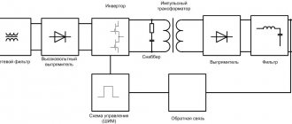
Generalized block diagram of a pulse power supply.
Switching power supplies are built on a different principle. Since the current consumed is sharply non-sinusoidal, a filter is installed at the input. It does not affect the performance of the unit in any way, which is why many industrial manufacturers of Economy class power supplies do not install it. You don’t have to install it in a simple homemade source, but this will lead to the fact that devices on microcontrollers powered by the same 220 volt network will begin to fail or work unpredictably.
Then the mains voltage is straightened and smoothed out. An inverter using transistor switches in the primary winding circuit of the transformer creates pulses with an amplitude of 220 volts and a high frequency - up to several tens of kilohertz, in contrast to 50 hertz in the network. Due to this, the power transformer is compact and lightweight. The secondary winding voltage is rectified and filtered. Due to the high conversion frequency, smaller capacitors can be used here, which has a positive effect on the dimensions of the device. Also, in high-frequency voltage filters, it becomes advisable to use chokes - small-sized inductors effectively smooth out HF pulsations.
Voltage regulation and current limitation are performed through feedback circuits, which are supplied with voltage from the source output. If, due to an increase in load, the voltage begins to decrease, then the control circuit increases the interval of the open state of the keys without reducing the frequency (pulse width control method). If the voltage needs to be reduced (including to limit the output current), the time the switches are open is reduced.
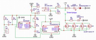
Printed circuit board
The printed circuit board has dimensions of 72x75mm. It was taken from a forum thread on the development of PiDBP. The board is wired without a rectifier and filter capacitors, that is, only the stabilizer itself.
The pin numbers of the channels of the DA1 microcircuit on the diagram and the printed circuit board are different; more precisely, the channels are connected according to the principle of wiring the printed circuit board (both simpler and connected). In general, it makes no difference which of the four channels will be DA1.1, and which will be DA1.2, and so on, the main thing is to follow the connection diagram.
For convenience, installation must begin with jumpers and resistors.
Next, all other components are mounted, from smallest to largest.
How to select components
For a transformer source, first of all, a transformer is selected. In most cases, it is taken ready-made from what is available. This node must produce the required current at maximum voltage. The combination of these parameters is ensured by the overall power of the transformer. For industrial devices, parameters can be found in the reference book. For random transformers, the power can be determined by the core dimensions (in centimeters).
Core area for different types of transformers.
Power is calculated using the formula:
P=S2/1.44 where:
- P-power in Watts;
- S is the cross section in square centimeters.
For practical purposes, the power must also be multiplied by the efficiency. For example, a transformer with a core area of 6 sq.cm. at a voltage of 35 volts and a stabilizer output voltage of 30 volts (the overall efficiency can be taken as 0.75) it is capable of delivering power P=(36/1.44)*0.75=18.75 watts. The maximum current will be I=P/U=18.75/35=0.5 A.
If the transformer passes power, but the secondary winding is designed for a different voltage, it can be removed and a new one wound (if it fits). The number of turns is calculated as follows:
- the number of turns per volt is determined by the formula 50/S, where S is the core area in sq.cm;
- this value is multiplied by the required voltage level.
So, for an area of 6 cm per 1 volt there are 50/6 = 8.3 turns per volt. For a voltage of 35 volts, the winding must have 35 * 8.3 = 291 turns. The wire diameter is calculated using the formula D=0.02, where I is the current in milliamps. For a current of 5 amperes, you need to take a wire with a diameter of 0.02 * = 70 * 0.02 = 1.4 mm.
If a high-power transistor is selected for a linear regulator, the main criterion for application is the collector current. It must cover the load current with a margin. This parameter for common domestic and foreign transistors is given in the table.
| Transistor | Maximum collector current (constant), A |
| KT818 (819) | 10 |
| KT825 (827) | 20 |
| KT805 | 5 |
| TIP36 | 25 |
| 2N3055 | 15 |
| MJE13009 | 12 |
When operating in modes close to the maximum current, transistors must be installed on radiators.
You also need to pay attention to such a parameter as the maximum voltage between the collector and emitter. With an input voltage of 35 volts and an output voltage of 1.5, the difference will be 33.5 volts; for some semiconductor devices this is unacceptable.
The capacity of the oxide capacitor located after the rectifier is selected based on the load. There are formulas for calculating filter parameters, but in practice the approach is simple: the more, the better. There are two restrictions imposed on the capacity:
- capacitor dimensions;
- inrush current per charge, which can be significant with a large capacity.
The output capacitor of the power supply can have a capacity of about 1000 µF.
Cooling
The VT2 housing needs to be cooled. The heat sink must be installed outside the power supply case for effective natural convection, or active (forced) cooling must be used. For passive cooling, I recommend choosing a radiator area of 10-20 cm2 per 1 W of transistor power dissipation, which is equal to P = (Uin-Uout) × Iload. If you plan to work with a load for a long time, then we take 20 cm2 per 1 W, and if the LBP will be used only for checking or starting devices, then you can get by with 10 cm2 per 1 W.
Laboratory power supply circuits
On the Internet you can find many diagrams of laboratory power supplies. The choice is determined based on the tasks, the qualifications of the technician and the availability of components.
Switching power supply on tl494
The TL494 chip is iconic in the field of switching power supplies. Most power supplies of desktop computers are made on its basis.
Pinout and pin assignment of TL494.
Based on the TL494, you can also make a laboratory source in accordance with the structure discussed above.
Switching power supply circuit on TL494.
A surge filter is installed at the input of the unit. After it there is a high-voltage rectifier on VDS1 (you can use any assemblies and diodes for the appropriate voltage), which generates a constant voltage of 220 volts. An auxiliary transformer TR3 with a rectifier VDS2 is connected in parallel to the rectifier. These elements generate +12 volts to power the microcircuits. TL494 generates a sequence of pulses, the frequency of which is determined by the C3R3 chain. The signal is amplified by switches on transistors T1, T2 and through transformer TR1 is supplied to bases T3, T4. These powerful transistors form high-voltage pulses in the primary winding of transformer TR2. Pulses with a repetition rate of several tens of kilohertz are transformed into the secondary winding of the transformer, rectified by the D5 assembly, filtered and supplied to the consumer.
The voltage feedback circuit is formed on elements OP3, OP4 of the operational amplifier. Resistor R15 sets the required output level. The actual current is measured as the voltage drop across the shunt of resistors R25, R26. Elements OP1, OP2 create a circuit for limiting the maximum current (the required value is set by a potentiometer). The TL494 microcircuit, depending on the specified current and voltage, increases or decreases the duration of the open state of the keys. Transistors T3, T4, as well as diode D5 must be installed on radiators. It is highly desirable to organize forced airflow of circuit elements. The fan can be connected to a DC voltage source of +12 volts.
The ratings and types of elements are shown in the diagram. Many components, including winding elements, can be taken from a faulty or unnecessary computer power supply. Choke L5 is wound on a yellow toroidal core and contains 50 turns of wire with a diameter of 1.5 mm.
Power supply with switching stabilizer.
Another option for using the TL494 chip is in a pulse stabilizer for a power supply, made according to a “transformer” circuit. This source produces voltage from 0 to 30 volts at a current of up to 5 amperes.
Here the microcircuit controls the opening and closing of the key on transistor VT1. In the open state, energy is accumulated in the throttle L1, in the closed state it is transferred from the throttle to the consumer. Diode VD1 “eats” the negative voltage pulse that occurs when switching a circuit with high inductance.
The greater the load, the faster the energy in the inductance is consumed, the faster the voltage on capacitor C4 drops, the longer the transistor must be opened. The feedback voltage is supplied to the microcircuit from the potentiometer R9. They set the required output level. The current is measured as the voltage drop across shunt R12. The required current limit level is set using R3.
The circuit section containing the LM358 operational amplifier and the K155LA3 logic chip (it is better to use the K555LA3) serves to indicate the power supply mode - current stabilization or voltage stabilization.
Resistors R4 and R10, designed for precise adjustment of voltage and current, can be omitted - in practice they are of no use. During assembly, it is necessary to ensure effective cooling of the elements:
- transistor VT1;
- diode VD1;
- throttle L1;
- shunt R12.
The use of a cooler is highly recommended. Instruments should also be installed to indicate the current current and voltage values.
We recommend trying: Converting a computer power supply into a laboratory power supply with voltage regulation
On a p210 transistor
P210 transistors have been preserved in the storage rooms of many radio amateurs. It is not so easy to find applications for them - more modern components have appeared, their frequency characteristics and gain leave the outdated device far behind. But one parameter - the maximum collector current of the P210, which is 12 A when installed on a radiator - allows them to be used today in regulated power supplies.
The circuit is simple, but you need to pay attention that the transistor is connected to the negative arm (P210 has a pnp structure). The capacitor after the rectifier must have a capacity of at least 5000 μF, and at the output - at least 1000 μF. P210 can have a low gain, so transistor VT2 is added to it - any low-power pnp structure.
Power supply circuit using transistor P210 or similar.
The source can use a transformer TN-36-127/220-50, which has 4 secondary windings of 6.3 volts each. By connecting two of them in series, you can build a homemade power supply with an output voltage of up to 12 V, and if you connect 4 windings in the same way - up to 24 V. You can also use other step-down transformers that are suitable for current and voltage.
Connection diagram of TN-36-127/220-50 windings.
Similar controlled voltage sources can be built using other transistors, including npn. In this case, the power element is included in the positive arm of the power supply unit.
Power supply based on transistor KT829.
These simple power supplies do not have short circuit or overload protection. It is highly advisable to install a voltmeter and an ammeter at the output to monitor the mode. The transistor must be installed on the radiator.
On lm317
Using the LM317 chip, you can assemble a power supply with a linear voltage regulator and adjustable current limit. The main advantage of this microcircuit is its simple connection circuit with a minimum of wiring. The standard connection diagram looks like this:
Standard connection circuit LM317.
The output voltage is set by the divider R1R2. By changing the output voltage, the microcircuit tries to hold the current through the divider so that the voltage drop across R1 is 1.25 volts. Therefore, the larger R2, the greater the output voltage. If you replace R2 with a potentiometer, the output voltage can be adjusted. The output level is calculated using the formula Uout=1.25*(1+R2/R1).
If R2 = 0, then the output will be 1.25 volts - this is the minimum possible voltage for this connection.
On the Internet there are many circuits on the LM317 with voltage regulation from zero volts (including applying a negative bias to the Adjust pin). Most of these technical solutions only work on paper.
In the datasheet for the chip there is such a connection diagram.
This is enough to build a simple adjustable laboratory, but there is a problem. The microcircuit in such a connection produces no more than 1.5 A, even if it is installed on a radiator. The second disadvantage is that in order to get an output voltage of 30 V, about 35 VDC must be applied to the input. If it is necessary to obtain an output level close to the minimum, restrictions on the maximum power dissipation come into effect - with a differential of 35/1.25, the maximum current can be 0.3..0.5 A (depending on the microcircuit package). This is very little. Therefore, the microcircuit must be powered with an external transistor.
The manufacturer offers such a scheme.
As an external one, you can use a domestic transistor of the pnp structure KT818 with the letter index B-G (KT818A may not pass the collector-emitter voltage). If it is installed on a radiator, the maximum current in theory will be 10 A, but this is if there are no restrictions on the current of the rectifier diodes and the power of the transformer.
Power transistors of the NPN structure are more common. If you need to power up the stabilizer with such an element, you can use the circuit from the datasheet.
Using a powerful npn element recommended by the chip developer.
Here, a low-power pnp transistor is used (you can use the domestic KT814), which controls a powerful npn element (for example, KT819).
Often used in practice, the use of a powerful npn element.
But more often a switch is used that is not provided for by the developer - the transistor is switched on by the base to the output of the microcircuit.
Each of the proposed circuits can be used as a laboratory power supply on the LM317, but in practice the LBP circuit, supplemented by maximum current adjustment, is popular.
Power supply circuit for LM317.
The device is powered by a mains transformer with two windings. The additional winding serves to create a negative power arm of the op-amp LM301, on which the current limiting circuit is assembled. The operational amplifier is connected according to a comparator circuit - on one pin there is a reference voltage, regulated using P1, on the other - the voltage created by the actual current on the shunt resistor R5.
If the actual current exceeds the set current, the state at the output of the comparator changes to the opposite. The LED lights up and the voltage is limited to a level that maintains the set current value.
Based on this circuit, a stationary power supply is assembled, providing two voltage channels with regulation of 1.25..30 volts and current limitation within 5A for each channel.
Appearance of the power supply.
If necessary, the channels can be connected in series to a common point - a bipolar source will be obtained. 90+ percent of components and materials, including the housing, can usually be found in the storage rooms of any radio amateur.
Internal layout of the power supply.
The unit is assembled in a housing from a faulty frequency response meter “Test”. Power transformers of unknown origin were used, suitable in power and voltage (one had to rewind the secondary winding to obtain a voltage of 35 volts). There was not enough space on it for an additional winding, so the negative arm of one of the channels is powered from a separate small transformer.
Stabilizer printed circuit board.
Most of the elements are located on the boards; the drawing and location of the parts can be found on the Internet. You can design and manufacture your own board.
Recommended printed circuit board design and arrangement of elements on it.
The measurement scheme has been changed - voltmeter-ammeter blocks have been used, which can be purchased on trading platforms on the Internet. Elements R8, R9, P4 and an analog voltmeter do not need to be installed in this version. The output transistors are installed on radiators located on the rear wall of the case. The rectifier diodes are installed on homemade radiators.
The domestic analogue of LM317 is the 142EN12A microcircuit.
During setup, the power supply was loaded with car light bulbs up to a current of 5 A, and the trimming resistor P1 (at maximum resistance P2) set the protection to trigger.
The circuit proved to be efficient, although the current limiting does not work according to the best algorithm. When the current goes beyond the limits, the voltage simply drops to a minimum. It is better to find a circuit that in this case switches the power supply to current stabilization mode. If you need a higher voltage LPS (with an output level of up to 60 volts), it can be made on the LM317HV chip and use transformers with the appropriate voltage.
On lt1083
Instead of the LM317 chip, you can use the LT1083. Its specific differences:
- low voltage drop (at maximum current no more than 1.5 V);
- increased output current.
The first advantage leads to the fact that less power will be dissipated on the microcircuit, therefore, at low voltage values, increased current can be removed from it. In addition, the output voltage of the transformer can be made lower (not much, by 1..2 volts, but sometimes this is critical).
The second advantage leads to the fact that in many cases you can do without an external powerful transistor. The maximum current supplied by the LT108X series stabilizers is shown in the table.
| Chip | Maximum current, A |
| LT1083 | 3 |
| LT1084 | 5 |
| LT1085 | 7,5 |
A current of 7.5 amperes covers 90+ percent of the needs of a home laboratory. Otherwise, regarding the topic of the review, the circuit does not differ from the circuit on the LM317.
Pinout and typical connection diagram for linear stabilizers of the LT108X series.
Article on the topic: Computer power supply circuits - complete description with examples