Printed circuit board
– this is a dielectric base, on the surface and in the volume of which conductive paths are applied in accordance with the electrical circuit. The printed circuit board is intended for mechanical fastening and electrical connection between the leads of electronic and electrical products installed on it by soldering.
The operations of cutting out a workpiece from fiberglass, drilling holes and etching a printed circuit board to obtain current-carrying tracks, regardless of the method of applying the pattern to the printed circuit board, are performed using the same technology.
Manual method of applying PCB tracks
Preparing the template
The paper on which the printed circuit board layout is drawn is usually thin and for more accurate drilling of holes, especially when using a hand-made homemade drill, so that the drill does not lead to the side, it is necessary to make it thicker. To do this, you need to glue the printed circuit board design onto thicker paper or thin thick cardboard using any glue, such as PVA or Moment.
Next, the thick paper is cut out along the contour of the glued pattern and the template for drilling is ready.
Cutting the workpiece
A blank of foil fiberglass laminate of a suitable size is selected, the printed circuit board template is applied to the blank and outlined around the perimeter with a marker, a soft pencil or marking with a sharp object.
Next, the fiberglass laminate is cut along the marked lines using metal scissors or sawed out with a hacksaw. Scissors cut faster and there is no dust. But we must take into account that when cutting with scissors, fiberglass is strongly bent, which somewhat worsens the adhesion strength of copper foil and if the elements need to be re-soldered, the tracks may peel off. Therefore, if the board is large and has very thin traces, then it is better to cut it using a hacksaw.
The template of the printed circuit board pattern is glued to the cut-out workpiece using Moment glue, four drops of which are applied to the corners of the workpiece.
Since the glue sets in just a few minutes, you can immediately begin drilling holes for radio components.
Where can I buy
Where can you buy foil-coated PCB? Yes, by the way, not only textolite, but also other tools for amateur radio creativity.
Currently, I don’t have any problems with this, since there are several decent radio stores in my city. There I buy textolite and everything I need.
At one time, when there was no normal radio store in my city, I ordered all the materials, tools and radio parts from the online store. One of these online stores where you can find textolite and not only this is the Dessie store, by the way, I even wrote an article about it.
Drilling holes
It is best to drill holes using a special mini drilling machine with a carbide drill with a diameter of 0.7-0.8 mm. If a mini drilling machine is not available, then you can drill holes with a low-power drill using a simple drill. But when working with a universal hand drill, the number of broken drills will depend on the hardness of your hand. You definitely won’t be able to get by with just one drill.
If you cannot clamp the drill, you can wrap its shank with several layers of paper or one layer of sandpaper. You can wrap a thin metal wire tightly around the shank, turn to turn.
After finishing drilling, check whether all holes are drilled. This can be clearly seen if you look at the printed circuit board up to the light. As you can see, there are no missing holes.
Applying a topographic drawing
In order to protect the places of foil on fiberglass laminate that will be conductive paths from destruction during etching, they must be covered with a mask that is resistant to dissolution in an aqueous solution. For the convenience of drawing paths, it is better to pre-mark them using a soft pencil or marker.
Before applying the markings, it is necessary to remove traces of the glue that was used to glue the printed circuit board template. Since the glue has not hardened much, it can be easily removed by rolling it with your finger. The surface of the foil must also be degreased using a rag using any means, such as acetone or white alcohol (the so-called purified gasoline), or any dishwashing detergent, for example Ferry.
After marking the tracks of the printed circuit board, you can begin to apply their design. Any waterproof enamel is well suited for drawing paths, for example alkyd enamel of the PF series, diluted to a suitable consistency with a white alcohol solvent. You can draw paths with different tools - a glass or metal drawing pen, a medical needle, and even a toothpick. In this article I will tell you how to draw circuit board traces using a drawing pen and ballerina, which are designed for drawing on paper with ink.
Previously, there were no computers and all drawings were drawn with simple pencils on whatman paper and then transferred in ink to tracing paper, from which copies were made using copiers.
Drawing begins with contact pads, which are drawn with a ballerina. To do this, you need to adjust the gap of the sliding jaws of the ballerina drawing board to the required line width and to set the diameter of the circle, perform the adjustment with the second screw, moving the drawing blade away from the axis of rotation.
Next, the ballerina's drawing board is filled with paint to a length of 5-10 mm using a brush. For applying a protective layer to a printed circuit board, PF or GF paint is best suited, since it dries slowly and allows you to work quietly. NTs brand paint can also be used, but it is difficult to work with because it dries quickly. The paint should adhere well and not spread. Before painting, the paint must be diluted to a liquid consistency, adding a suitable solvent to it little by little with vigorous stirring and trying to paint on scraps of fiberglass. To work with paint, it is most convenient to pour it into a bottle of manicure varnish, in the twist of which there is a solvent-resistant brush installed.
After adjusting the ballerina's drawing board and obtaining the required line parameters, you can begin to apply the contact pads. To do this, the sharp part of the axis is inserted into the hole and the base of the ballerina is rotated in a circle.
With the correct setting of the drawing pen and the desired consistency of paint around the holes on the printed circuit board, perfectly round circles are obtained. When a ballerina begins to paint poorly, the remaining dried paint is removed from the gap of the drawing board with a cloth and the drawing board is filled with fresh paint. To draw all the holes on this printed circuit board with circles it took only two refills of the drawing pen and no more than two minutes of time.
Once the round pads on the board are drawn, you can start drawing the conductive paths using a hand drawing pen. Preparing and adjusting a manual drawing board is no different from preparing a ballerina.
The only thing additionally needed is a flat ruler, with pieces of rubber 2.5-3 mm thick glued to one of its sides along the edges, so that the ruler does not slip during operation and the fiberglass, without touching the ruler, can freely pass under it. A wooden triangle is best suited as a ruler; it is stable and at the same time can serve as a hand support when drawing a printed circuit board.
To prevent the printed circuit board from slipping when drawing tracks, it is advisable to place it on a sheet of sandpaper, which consists of two sandpaper sheets sealed together with the paper sides.
If they come into contact when drawing paths and circles, then you should not take any measures. You need to let the paint on the printed circuit board dry until it does not stain when touched, and use the tip of a knife to remove the excess part of the design. In order for the paint to dry faster, the board should be placed in a warm place, for example, on a radiator in winter. In the summer - under the rays of the sun.
When the design on the printed circuit board is completely applied and all defects are corrected, you can proceed to etching it.
Equipment
Different development boards are equipped with a different set of additional elements. Expensive models are equipped with a set of jumper wires; they are useful for connecting parts with thick leads, more than 0.7 mm in diameter, to the device. The connecting wires included in the kit can be of different lengths.
The set can be equipped with additional connectors and other useful items. This allows you to effortlessly assemble the most complex projects in the shortest possible time. The kit may also include a power supply, which is necessary to test the functionality of the assembled circuit.
Technology of applying a printed circuit board pattern using a laser printer
When printing on a laser printer, the image formed by the toner is transferred, due to electrostatics, from the photo drum on which the laser beam drew the image, onto paper. The toner is held onto the paper, preserving the image, only due to electrostatics. To fix the toner, the paper is rolled between rollers, one of which is a thermal oven heated to a temperature of 180-220°C. The toner melts and penetrates the paper texture. Once cooled, the toner hardens and adheres firmly to the paper. If the paper is heated again to 180-220°C, the toner will again become liquid. This property of toner is used to transfer images of current-carrying tracks onto a printed circuit board at home.
After the file with the printed circuit board design is ready, you need to print it using a laser printer onto paper. Please note that the image of the printed circuit board drawing for this technology must be viewed from the side where the parts are installed!
An inkjet printer is not suitable for these purposes, as it works on a different principle.
Preparing a paper template for transferring the design to the printed circuit board
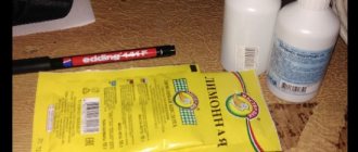
If you print a printed circuit board design on ordinary paper for office equipment, then due to its porous structure, the toner will penetrate deeply into the body of the paper and when the toner is transferred to the printed circuit board, most of it will remain in the paper. In addition, there will be difficulties in removing paper from the printed circuit board. You will have to soak it in water for a long time. Therefore, to prepare a photomask, you need paper that does not have a porous structure, for example, photo paper, backing from self-adhesive films and labels, tracing paper, pages from glossy magazines.
I use old stock tracing paper as the paper for printing the PCB design. Tracing paper is very thin and it is impossible to print a template directly on it; it gets jammed in the printer. To solve this problem, before printing, you need to apply a drop of any glue to a piece of tracing paper of the required size in the corners and glue it to a sheet of A4 office paper.
This technique allows you to print a printed circuit board design even on the thinnest paper or film. In order for the toner thickness of the drawing to be maximum, before printing, you need to configure the “Printer Properties” by turning off the economical printing mode, and if this function is not available, then select the coarsest type of paper, for example cardboard or something similar. It’s entirely possible that you won’t get a good print the first time, and you’ll have to experiment a little to find the best print mode for your laser printer. In the resulting print of the design, the tracks and contact pads of the printed circuit board must be dense without gaps or smudging, since retouching at this technological stage is useless.
All that remains is to cut the tracing paper along the contour and the template for making the printed circuit board will be ready and you can proceed to the next step, transferring the image onto fiberglass laminate.
Transferring a design from paper to fiberglass
Transferring the printed circuit board design is the most critical step. The essence of the technology is simple: paper, with the side of the printed pattern of the tracks of the printed circuit board, is applied to the copper foil of fiberglass and pressed with great force. Next, this sandwich is heated to a temperature of 180-220°C and then cooled to room temperature. The paper is torn off, and the design remains on the printed circuit board.
Some craftsmen suggest transferring a design from paper to a printed circuit board using an electric iron. I tried this method, but the result was unstable. It is difficult to simultaneously ensure that the toner is heated to the required temperature and that the paper is pressed evenly onto the entire surface of the printed circuit board when the toner hardens. As a result, the pattern is not completely transferred and gaps remain in the pattern of the printed circuit board tracks. Perhaps the iron was not heating up enough, although the regulator was set to maximum iron heating. I didn’t want to open the iron and reconfigure the thermostat. Therefore, I used another technology, less labor-intensive and providing one hundred percent results.
On a piece of foil fiberglass laminate cut to the size of the printed circuit board and degreased with acetone, I glued tracing paper with a pattern printed on it in the corners. On top of the tracing paper I placed, for more even pressure, heels of sheets of office paper. The resulting package was placed on a sheet of plywood and covered on top with a sheet of the same size. This entire sandwich was clamped with maximum force in clamps.
All that remains is to heat the prepared sandwich to a temperature of 200°C and cool. An electric oven with a temperature controller is ideal for heating. It is enough to place the created structure in a cabinet, wait for the set temperature to reach, and after half an hour remove the board to cool.
If you don’t have an electric oven, you can use a gas oven by adjusting the temperature using the gas supply knob using the built-in thermometer. If there is no thermometer or it is faulty, then women can help; the position of the control knob at which pies are baked is suitable.
Since the ends of the plywood were warped, I clamped them with additional clamps just in case. To avoid this phenomenon, it is better to clamp the printed circuit board between metal sheets 5-6 mm thick. You can drill holes in their corners and clamp printed circuit boards, tighten the plates using screws and nuts. M10 will be enough.
After half an hour, the structure has cooled enough for the toner to harden, and the board can be removed. At the first glance at the removed printed circuit board, it becomes clear that the toner transferred from tracing paper to the board perfectly. The tracing paper fit tightly and evenly along the lines of the printed tracks, rings of contact pads and marking letters.
The tracing paper easily came off from almost all the traces of the printed circuit board; the remaining tracing paper was removed with a damp cloth. But still, there were gaps in several places on the printed tracks. This can happen as a result of uneven printing from the printer or remaining dirt or corrosion on the fiberglass foil. Gaps can be painted over with any waterproof paint, manicure polish, or retouched with a marker.
To check the suitability of a marker for retouching a printed circuit board, you need to draw lines on paper with it and moisten the paper with water. If the lines do not blur, then the retouching marker is suitable.
It is best to etch a printed circuit board at home in a solution of ferric chloride or hydrogen peroxide with citric acid. After etching, toner can be easily removed from the printed tracks with a swab soaked in acetone.
Then holes are drilled, conductive paths and contact pads are tinned, and radioelements are sealed.
This is the appearance of the printed circuit board with radio components installed on it. The result is a power supply and switching unit for an electronic system that complements an ordinary toilet with a bidet function.
Connecting wires
If the board does not come with connecting wires, you can use regular ones. They must be insulated, then you can safely assemble any circuit diagram.
The wires most often used for such purposes are those used in security alarms. Any single-core or stranded wires will also work. The main thing is that it is convenient to work with them. All you need to do is cut the wire into pieces of the required length and strip their ends of insulation. It is advisable to tin all ends.
PCB etching
To remove copper foil from unprotected areas of foiled fiberglass laminate when making printed circuit boards at home, radio amateurs usually use a chemical method. The printed circuit board is placed in an etching solution and, due to a chemical reaction, the copper unprotected by the mask dissolves.
Recipes for pickling solutions
Depending on the availability of components, radio amateurs use one of the solutions given in the table below. Etching solutions are arranged in order of popularity of their use by radio amateurs at home.
| Name of solution | Compound | Quantity | Cooking technology | Advantages | Flaws |
| Hydrogen peroxide plus citric acid | Hydrogen peroxide (H2O2) | 100 ml | Dissolve citric acid and table salt in a 3% solution of hydrogen peroxide. | Availability of components, high etching speed, safety | Not stored |
| Citric acid (C6H8O7) | 30 g | ||||
| Table salt (NaCl) | 5 g | ||||
| Aqueous solution of ferric chloride | Water (H2O) | 300 ml | Dissolve ferric chloride in warm water | Sufficient etching speed, reusable | Low availability of ferric chloride |
| Ferric chloride (FeCl3) | 100 g | ||||
| Hydrogen peroxide plus hydrochloric acid | Hydrogen peroxide (H2O2) | 200 ml | Pour 10% hydrochloric acid into a 3% hydrogen peroxide solution. | High etching rate, reusable | Great care required |
| Hydrochloric acid (HCl) | 200 ml | ||||
| Aqueous solution of copper sulfate | Water (H2O) | 500 ml | Dissolve table salt in hot water (50-80°C), and then copper sulfate | Component Availability | The toxicity of copper sulfate and slow etching, up to 4 hours |
| Copper sulfate (CuSO4) | 50 g | ||||
| Table salt (NaCl) | 100 g |
Etching printed circuit boards in metal containers is not allowed.
. To do this, you need to use a container made of glass, ceramic or plastic. The used etching solution may be disposed of in the sewer system.
Etching solution of hydrogen peroxide and citric acid
A solution based on hydrogen peroxide with citric acid dissolved in it is the safest, most affordable and fastest working. Of all the solutions listed, this is the best by all criteria.
Hydrogen peroxide can be purchased at any pharmacy. Sold in the form of a liquid 3% solution or tablets called hydroperite. To obtain a liquid 3% solution of hydrogen peroxide from hydroperite, you need to dissolve 6 tablets weighing 1.5 grams in 100 ml of water.
Citric acid in the form of crystals is sold in any grocery store, packaged in bags weighing 30 or 50 grams. Table salt can be found in any home. 100 ml of etching solution is enough to remove 35 microns thick copper foil from a 100 cm2 printed circuit board. The used solution is not stored and cannot be reused. By the way, citric acid can be replaced with acetic acid, but because of its pungent odor, you will have to etch the printed circuit board outdoors.
Ferric chloride pickling solution
The second most popular etching solution is an aqueous solution of ferric chloride. Previously, it was the most popular, since ferric chloride was easy to obtain at any industrial enterprise.
The etching solution is not demanding on temperature; it etches quickly enough, but the etching rate decreases as the ferric chloride in the solution is consumed.
Ferric chloride is very hygroscopic and therefore quickly absorbs water from the air. As a result, a yellow liquid appears at the bottom of the jar. This does not affect the quality of the component and such ferric chloride is suitable for preparing an etching solution.
If the used ferric chloride solution is stored in an airtight container, it can be reused many times. Subject to regeneration, just pour iron nails into the solution (they will immediately be covered with a loose layer of copper). If it gets on any surface, it leaves hard-to-remove yellow stains. Currently, ferric chloride solution is used less frequently for the manufacture of printed circuit boards due to its high cost.
Etching solution based on hydrogen peroxide and hydrochloric acid
Excellent etching solution, provides high etching speed. Hydrochloric acid, with vigorous stirring, is poured into a 3% aqueous solution of hydrogen peroxide in a thin stream. It is unacceptable to pour hydrogen peroxide into acid! But due to the presence of hydrochloric acid in the etching solution, great care must be taken when etching the board, since the solution corrodes the skin of the hands and spoils everything it comes into contact with. For this reason, it is not recommended to use an etching solution with hydrochloric acid at home.
Etching solution based on copper sulfate
The method of manufacturing printed circuit boards using copper sulfate is usually used if it is impossible to produce an etching solution based on other components due to their inaccessibility. Copper sulfate is a pesticide and is widely used for pest control in agriculture. In addition, the etching time of the printed circuit board is up to 4 hours, while it is necessary to maintain the solution temperature at 50-80°C and ensure a constant change of the solution at the surface being etched.
PCB etching technology
For etching the board in any of the above etching solutions, glass, ceramic or plastic dishes, for example from dairy products, are suitable. If you don’t have a suitable container size at hand, you can take any box made of thick paper or cardboard of a suitable size and line its inside with plastic wrap. An etching solution is poured into the container and a printed circuit board is carefully placed on its surface, pattern down. Due to the forces of surface tension of the liquid and its light weight, the board will float.
For convenience, you can glue a plastic bottle cap to the center of the board with instant glue. The cork will simultaneously serve as a handle and a float. But there is a danger that air bubbles will form on the board and the copper will not be etched in these places.
To ensure uniform etching of copper, you can place the printed circuit board on the bottom of the container with the pattern facing up and periodically shake the tray with your hand. After some time, depending on the etching solution, areas without copper will begin to appear, and then the copper will completely dissolve on the entire surface of the printed circuit board.
After the copper is completely dissolved in the etching solution, the printed circuit board is removed from the bath and thoroughly washed under running water. Toner is removed from the tracks with a rag soaked in acetone, and paint is easily removed with a rag soaked in a solvent that was added to the paint to obtain the desired consistency.
Preparing the printed circuit board for installation of radio components
The next step is to prepare the printed circuit board for the installation of radio elements. After removing the paint from the board, the tracks need to be sanded in a circular motion with fine sandpaper. There is no need to get carried away, because the copper tracks are thin and can be easily ground off. Just a few passes with abrasive with light pressure are enough.
Next, the current-carrying paths and contact pads of the printed circuit board are coated with alcohol-rosin flux and tinned with soft solder using an electric soldering iron. To prevent the holes on the printed circuit board from being covered with solder, you need to take a little bit of it onto the soldering iron tip.
After completing the manufacture of the printed circuit board, all that remains is to insert the radio components into the designated positions and solder their leads to the pads. Before soldering, the legs of the parts must be moistened with alcohol-rosin flux. If the legs of the radio components are long, then before soldering they need to be cut with side cutters to a protrusion length above the surface of the printed circuit board of 1-1.5 mm. After completing the installation of parts, you need to remove any remaining rosin using any solvent - alcohol, white alcohol or acetone. They all successfully dissolve rosin.
You can learn more about soldering technology using examples of soldering parts, brands of solders and fluxes, design and repair of soldering irons from the series of articles in the section “How to solder with a soldering iron.”
It took no more than five hours to implement this simple capacitive relay circuit from laying out the tracks for manufacturing a printed circuit board to creating a working sample, much less than it took to type up this page.
Errors during production
Common mistakes include overheating the board and poor etching solution. Always mix all the components of the solution, otherwise it will not begin to etch the board. Soldering acid should not be used when tinning the board. It will damage the board over time if you don't clean it well.
Some radio amateurs also have the practice of tinning boards with Rose alloy. You should not do this, since such an alloy is intended for desoldering parts, and not for permanent soldering. In addition, it is fragile and will quickly oxidize over time.