General principles of multivibrator operation
As stated in the encyclopedia, “a symmetrical multivibrator is a two-stage amplifier covered by positive feedback.” Let's look at the diagram:
Rice. 1. Two-stage amplifier with positive feedback
If you have read the article about the amplifier stage on a transistor, then all the characters in this circuit are well known to you. This is a separating capacitor C, a base resistor Rb, which sets the bias current, and Rk as a load. And there are two such cascades here, they are absolutely identical.
What is unusual is the feedback wire (shown in red in the diagram), which closes our two-stage amplifier into a ring. It is thanks to positive feedback that our amplifier turns into an oscillator, controlling itself and maintaining undamped oscillations.
↑ Conclusion
Surface mounting provides tangible advantages not only for industrial use, but also for radio amateurs. It goes well with all types of traditional installation.
Practice shows that even replacing 5 - 20% of conventional elements with leadless SMDs gives a very noticeable gain. The manufacture of a printed circuit board is simplified and the installation density increases. The length of the signal conductors is reduced, which reduces parasitic inductance, capacitance and resistance, and in turn, leads to a significant improvement in the electrical parameters of the product.
From the materials of the portal forums it follows that radio amateurs use SMD parts when modifying finished products. And here the use of surface-mounted parts simplifies the task, since often there is no space left to install conventional elements.
An asymmetrical multivibrator using transistors of different structures serves as the basis for a lot of simple and useful designs [1 – 4, 7 – 14].
Despite the simplicity of the presented designs, their perfection should be noted, which is included in the epigraph of the publication.
Turning on the power
At the first moment after turning on the power, both transistors begin to open. Where does the opening current come from? Let's look at the example of transistor T1
Rice. 3. Power-on moment: currents that open the transistor
The first, obvious path is through Rb1, blue arrow in the figure. The second, not so obvious, is through capacitor C1. Let's not forget that at the first moment of time the capacitor is discharged, its resistance is practically zero, and a charge current appears in the circuit through Rк2 - C1 - emitter junction T1. This path is shown with a red arrow.
It is important to note here that the collector resistances Rк in this circuit are significantly less than the basic ones Rb, at least by an order of magnitude, or even several. This means that the “red” component will make a greater contribution at the first moment.
↑ Let's assemble the LM3909 chip on a discrete
The limiting factor to its popularity among hobbyists is the insufficient prevalence of the LM3909 chip and its inadequate price.
It is not difficult to make a prototype of a microcircuit, as suggested by a number of authors [1, 10, 11, 13]. At the same time, they provide very similar diagrams, practically copying the diagram from the manufacturer’s datasheet.
In Fig. Figure 9 shows a schematic diagram of a prototype LM3909 chip based on surface mount electronic components [14].
It should be remembered that the supply voltage range of the circuit is 1.5...6 V, and the zener diode VD1 (Fig. is not present in the collector circuit of transistor VT1.
As the resistance of resistor R1 increases, the duration of the flashes of LED HL1 increases, but their brightness decreases. The flash frequency is determined by the capacitance of capacitor C1 and the sum of the resistances of resistors R2 and R3.
Fight of transistors
However, both transistors do not have time to open completely. The fact is that, when opening, the transistor begins to interfere with its colleague. For example, as soon as T2 has a collector current, the potential on the right plate of C1 drops. In fact, the current through the capacitor begins to flow in the opposite direction: through Rb1 - C1 - collector junction T2:
Rice. 4. Direction of current through the opening transistor
It turns out that at the base of T1 the potential drops, T1 tends to close. But, closing, it accelerates the opening of T2, which leads to even greater locking of T1.
The same reasoning can be symmetrically applied to T2. That is, the transistors fight with each other, trying to open and at the same time close their neighbor.
Equilibrium does not occur here; in the end, one of the transistors necessarily wins and opens completely, going into saturation mode, while its colleague closes completely. The fact is that, even though our transistors are the same model, it is physically impossible to create two absolutely identical transistors. One of them will have a slightly higher gain, and this transistor will come out the winner. For definiteness, let us assume that T1 is closed and T2 is open.
Zenbuntu-desktop description and review
What is Zenbuntu-desktop? Zenbuntu-desktop is a Linux desktop variant for the Ubuntu Server operating system.
zenbuntu-desktop with default settings:
We list the programs and utilities available through the main menu of zenbuntu-desktop:
- Audio and video Music player
- Document View
- Zentual Administration
- Document View
- Activate ScreenSaver (Next)
- UXTerm
- Byobu Terminal
- Openbox Configuration Manager
- Switch off
- PCManFM File Manager
- LXTerminal
- Zentyal Administration
- Minimize windows
- System Monitor
- Time and calendar
- ScreenLock
- Shutdown
Source
Generation
All the processes described above occur very quickly, they are limited only by the speed of the transistors. After this, the circuit stabilizes and is in a stable state. However, this stability is only apparent, since some processes associated with the charge and discharge of capacitors continue:
Rice. 5. After switching transistors: fast charge C2 and slow charge C1
Firstly, capacitor C2 charges quite quickly - the resistance Rк1 is relatively small. In the figure, its charging path is shown with a red line.
If C2 has quickly charged and the current through it has stopped, what keeps T2 open? Answer: current through Rb2. This current, although less than through C2 at the first moment, is quite enough for the transistor to be completely open (in saturation mode).
Secondly, capacitor C1 also charges, but more slowly due to the relatively high resistance Rb1 - see the blue line in the figure. Note that the voltage on C1 is applied plus to the base of T1, and as C1 is charged, it increases. At some point (when the value reaches about 0.6 V), it will become sufficient to open T1, and this transistor will open.
And here C2 is waiting in ambush, already fully charged for a long time and tired from idleness. After T1 opens, it turns out that the entire accumulated potential of C2 is applied to the emitter junction of T2, and in the blocking polarity, which is why T2 instantly closes:
Rice. 6. When T1 opens, capacitor C2 closes T2
Explanation: The current does not flow along the red line, it only shows the direction of the potential. The fact is that the emitter junction T2 is blocked by this potential and its resistance is very high. Moreover, by closing, T2 accelerates the opening of T1, because the potential across its collector increases, and causes capacitor C1 to discharge even more through the emitter junction T1, opening it. What we get is an avalanche-like self-reinforcing process of simultaneous switching of transistors to the opposite state.
Well, then the events begin to repeat themselves symmetrically: C2 is slowly recharged in the opposite polarity, through Rb2 and the newly opened T1, until its potential becomes sufficient to open T2, and the transistors switch again, and so on.
↑ List of sources
1. Mosyagin V.V. Secrets of amateur radio skills. – M.: SOLON-Press. – 2005, 216 p. (pp. 47 – 64). 2. Shustov M.A. Practical circuit design. 450 useful diagrams for radio amateurs. Book 1. – M.: Altex-A, 2001. – 352 p. 3. Shustov M.A. Practical circuit design. Monitoring and protection of power supplies. Book 4. – M.: Altex-A, 2002. – 176 p. 4. Low-voltage flasher. (Abroad) // Radio, 1998, No. 6, p. 64. 5. Datagorsk article “The main tool is a soldering iron!” 6. Datasheet article “Soldering SMD parts at home” 7. Datasheet on LM3909 8. Shoemaker Ch. Amateur control and alarm circuits on ICs. – M:.Mir, 1989 (diagram 46. Simple low battery indicator, p. 104; diagram 47. Painter marker (flashing), p. 105). 9. Generator on LM3909 // Radio circuit, 2008, No. 2. 10. Nahrada obvodu LM3909 // Prakticka electronic A Radio, 2009, No. 6, p. 22. 11. Odinets A.L. Unusual application of LM3909 // Radioamator, 2009, No. 12, p. 16. 12. Borisevich K. IC LM3909 in amateur radio designs // Radiomir, 2010, No. 1, p. 19. 13. Discrete Version Of The LM3909 Oscillator IC 14. Belousov O.V. Equivalent of IC LM3909 on parts for surface mounting // Radioamator, 2011, No. 11, p. 34, 35.
Multivibrator frequency
Note that the charging of the capacitor through Rb continues for a relatively long time, but the switching of transistors occurs almost instantly. Therefore, the multivibrator generates rectangular pulses. And their frequency is determined by the charging time of the capacitors:
f = 1.443 / (C1*Rb1 + C2*Rb2)
where f is frequency (Hz), C is capacitance in farads, R is resistance in ohms
It remains to add a couple of technical notes. First: the multivibrator has two outputs, the signal can be removed from both the T1 collector and the T2 collector. These two signals are out of phase, some circuits take advantage of this property and use both signals. When connecting a load, it is important not to bypass the transistor, otherwise there is a risk of distorting the operation of the multivibrator, or even completely disrupting generation. It is best to connect the load in parallel with the collector resistance.
Well, the second note. It’s obvious, but without mentioning it, the article would be incomplete: we are analyzing here a circuit based on npn transistors, but in the same way, a multivibrator can be built on pnp transistors by changing the power polarity. And also on radio tubes, operational amplifiers, logic elements, etc. - the main thing is that there are two amplification stages covered by the OS. One of such schemes will be given below.
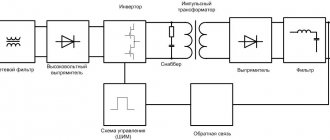
Voltage converter with a master oscillator based on an asymmetrical multivibrator
To obtain an output voltage of 30...80 V, P. Belyatsky [4.3] used a converter with a master oscillator based on an asymmetrical multivibrator with an output stage loaded on an inductive energy storage device - inductor (choke) L1 (Fig. 4.7).
Rice. 4.7. Circuit of a voltage converter with a master oscillator based on an asymmetrical multivibrator
The device is operational in the supply voltage range of 1.0... 1.5 V and has an efficiency of up to 75%.
In the circuit you can use a standard inductor DM-0.4-125
or another with an inductance of 120...200 μH.
A variant of the output stage of the voltage converter [4.4] is shown in Fig. 4.8. When a rectangular control signal cascade of TTL level (5 V) is applied to the input of the cascade, a voltage of 250 V is obtained at the output of the converter when it is powered from a 12 V source at a load current of 3...5 mA (load resistance is about 100 kOhm). Inductance of inductor L1 is 1 mH.
As VT1, you can use a domestic transistor, for example, KT604, KT605, KT704B, KT940A(B), KT969A, etc.
Rice. 4.8. Option for the output stage of the voltage converter
Rice. 4.9. Diagram of the output stage of the voltage converter
A similar output stage circuit (Fig. 4.9) made it possible, when powered from a source with a voltage of 28 V and a current consumption of 60 mA, to obtain an output voltage of 250 V at a load current of 5 mA [4.5]. The inductance of the choke is 600 μH. The frequency of control pulses is 1 kHz.
Depending on the quality of the inductor, the output voltage can be 150...450 V with a power of about 1 W and an efficiency of up to 75%.
The voltage converter [4.6], made on the basis of a pulse generator based on the DA1 KR1006VI1 (555) microcircuit, an amplifier based on a field-effect transistor VT1 and an inductive energy storage device with a rectifier and filter, is shown in Fig. 4.10.
At the output of the converter, with a supply voltage of 9 V and a current consumption of 80...90 mA, a voltage of 400...425 V is generated. It should be noted that the value of the output voltage is not guaranteed - it significantly depends on the method of constructing the inductor (choke) L1. For getting
Rice. 4.10. Circuit of a voltage converter with a pulse generator on a KR1006VI1 microcircuit
To obtain the desired voltage, the easiest way is to experimentally select an inductor to achieve the required voltage or use a voltage multiplier.
Source
Working circuit
To clearly demonstrate the operation of the multivibrator, I assembled a circuit on a breadboard. I placed an LED in series with Rk1 and Rk2.
The part numbers are as follows:
- T1, T2 - C1815
- Rk1, Rk2 - 1 kOhm
- Rb1, Rb2 - 47 kOhm
- C1, C2 - 10 µF (electrolytic, connected positive to the collector, negative to the base)
- Supply voltage - 5 V.
Rice. 7. Working multivibrator model
↑ SMD installation practice: let's make a talisman souvenir
Let's start mastering surface mounting using SMD components.
Let’s assemble a “flashing light” to use as a souvenir – a talisman. The printed circuit board and placement of elements of the light pulse generator are shown in Fig. 5. There are no holes in the board, and there is no power switch. You can turn off the power to the device by placing a small strip of paper between the GB1 battery terminal and the clamp terminal.
The small size of SMD components requires special care and accuracy during installation. You cannot do without a soldering iron with electronic temperature control, because overheating of the elements is completely unacceptable, as it will cause a loss of contact with the leads of the part.
Mastering surface mounting should be an incentive to purchase at least a simple soldering station and special tweezers (Fig. 6, 7).
The Hakko 937 soldering station belongs to the category of simple soldering stations and is perfect for beginner radio amateurs and household soldering work, as an excellent replacement for a regular soldering iron. This soldering station has small dimensions of 230×170*120 mm.
Alternative schemes
Let's look at several alternative circuits, as well as some ways to improve the performance of the multivibrator.
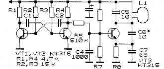
Multivibrators with adjustable frequency and duty cycle
Rice. 8. Multivibrator circuit with adjustable frequency (left) and duty cycle (right)
In the left circuit, due to the variable resistor, the values of Rb change, which means the frequency of the generator. On the right, the sum Rb1 + Rb2 remains unchanged, but the ratio of resistances in the base circuits changes. Thus, the frequency is fixed, but the duty cycle (the ratio of pulse length and pause) changes. Strictly speaking, this is already an asymmetrical multivibrator.
Multivibrator with improved waveform
If you carefully read the explanation of the operation of the multivibrator above, you remember that after switching the transistors, one of the capacitors is quickly recharged through the collector resistor Rk (see Fig. 5, red line). However, since the useful signal is removed precisely from the collector, the voltage changing on the capacitor introduces completely unnecessary interference into this signal. In the circuit in the following figure, an additional resistor is introduced, through which the same capacitor charge occurs:
Rice. 9. Separate the charging and discharging paths of capacitors: improving the signal shape
The capacitor is separated from the collector by a diode, which prevents the capacitor from distorting the front of the pulse at the moment the transistors are switched. But this same diode perfectly allows the capacitor to charge during the quasi-stable state of the multivibrator between switchings through Rb - diode - open transistor.
Multivibrator based on logical elements
Rice. 10. Multivibrator based on 2I-NOT elements
For an alternative logic multivibrator circuit, see this article.
Three-phase multivibrator
Rice. 11. Three-stage multivibrator circuit
Here, not two cascades are connected in series, but three. The circuit works in such a way that at any given time 2 transistors are open and one is closed. You can try to understand the operation of this circuit yourself, using the description of a symmetrical multivibrator above as a basis.
Rice. 12. Working model
Share on social networks:
Period calculation
Now you can calculate the oscillation period of the multivibrator.
According to Ohm's law, voltage V1 is equal to:
Let's transform this formula through conductivity:
V1 = Vs / ( 1 + R1||R3 / R2 ) = Vs / ( 1 + y2 / (y1 + y3) ) = Vs ( y1 + y3 ) / ( y1 + y2 + y3 )
If all resistances are equal, then V1 = (2 / 3) Vs
Then we find the voltage V0, it is equal to:
Let's transform this formula through conductivity:
V0 = Vs / (1 + R1 / R2||R3 ) = Vs / ( 1 + ( y2 + y3 ) / y1 ) = Vs y1 / ( y1 + y2 + y3 )
If all resistances are equal, then V0 = Vs / 3
When the comparator is switched, capacitor C discharges exponentially. The discharge time is equal to the charging time and is equal to half the period. Then:
Hence T = 2 RC ln( V1 / V0 ) = 2 RC ln[ ( y1 + y3 ) / y1 ]
Finally, the period of the multivibrator is equal to:
In the special case, if R1 = R3 period T = 1.386 RC
If R3 = 2 R1 period T= 0.811 RC
Text
DESCRIPTION 292222 IS COMPLETED BY THE AUTHOR'S CERTIFICATE Salus Soyetskiz Socialisticheskiy Respubliki Dependent on the author, certificate M IPC N 03 s 3/281 Declared 1.I.1969 (1339138/26-9) not before joining the Committee for Inventions and discoveries under the Council of Ministers of the USSRriori DK 621,373,43 (088.8) published on January 6, 1971, Bulletin Lr Date of publication isaniya 2.1 P.1971 Author's inventions Godho 3 applicant ULTIVIBRATOR WITH ADJUSTABLE FREQUENCY Multivibrators on transistors are known, in which frequency regulation is carried out by changing charging current capacitors with using triodes additionally connected to them. The disadvantage of these multivibrators is the strong dependence of the frequency on temperature fluctuations, which requires special measures for thermal stabilization, and a limited frequency control range. The purpose of the invention is to expand the frequency control range. This is achieved by the fact that the bases of the main triodes are connected to a control voltage source through zener diodes and collector-emitter junctions of control triodes, the bases of which are connected through resistors to the collectors of the triodes of the amplifier stages. The drawing shows a schematic diagram of the proposed multivibrator with adjustable frequency. The multivibrator contains generating transistors 1, 2; transistors 3, 4, facilitating fast charging of capacitors, transistors 5, b, acting as pulse amplifiers; cut-off transistors 7,8, connecting the control voltage source U, only to locked transistors 1 or 2, eliminating the influence of the control voltage on the degree of saturation of these transistors; timing capacitors 9, 10; timing resistances 11 - 14; silicon zener diodes 15, 1 b; diodes 17, 18, 5 cutting off the control circuit from the load; decoupling diodes 19, 20, making it possible to charge capacitors 9, 10 to the value of the supply voltage b resistance 21 - 24.10 When K. = O, transistor 1 opens, atransistor 2 is locked. At this time, transistor b is open, and transistors 5, 7 and 8 are locked. Timing capacitor 10 is charged through open transistor 4 and low-resistance resistance 22. Capacitor 9 is discharged. When it is discharged to zero, the circuit is transferred to another state. The multivibrator generates low frequency pulses.20 The circuit is symmetrical. If you increase the control voltage, then when transistor 1 is opened and transistor 2 is closed, transistor 7 is locked, and transistor 8 goes into a saturated state. Transistor 7 is closed, since transistor 5 is locked. At the first moment, capacitor 9 quickly discharges through zener diode 1 b, which gives time resistance 14 and saturated292222 Subject of invention haa Via Compiled by A. Merman Editor A. V. Korneev Technical editor A. A., Kamyshnikova Proofreaders: T. A. Abramova, A. Nikolaeva and L. Korogod Order 356/14 Circulation 473 Subscribed TsNIIPI Committee for Inventions and Discoveries prp Council of Ministers of the USSRMoscow, Zh, Raushskaya nab., 4,; 5 Printing house, Sapunova Ave., 2 transistor 8, and after locking the zener diode 1 b is discharged more slowly to zero through timing resistance 11. The minimum frequency of the operating range of regulation is determined by the value K, sufficient to transfer transistors 7 and 8 to a saturated state. This value is approximately 1 V. The frequency-angle dependence of the control potentiometer can be brought closer to linear if you use a potentiometer with an exponential characteristic. Diodes 17, 18 prevent the flow of control current into the load circuit when pulse amplifiers 5, 6 are locked. The frequency is adjusted by changing the discharge current of the capacitors. A multivibrator with an adjustable pulse frequency, containing the main generating 5 triodes with time-setting capacitive circuits and additional triodes, the emitters of which are through semiconductor diodes, and the bases are directly connected to the collectors of the main triodes, and the output axis 10 alloy cascades, characterized in that, in order to expand the frequency control range, the bases of the main triodes are connected to the control voltage source through zener diodes and collector-emitter junctions of the control triodes, the bases of which are connected through resistors to the collectors of the triodes of the amplifier stages,
- Bridge circuits
Look
Recommendations
- Jain, R.P.; Anand, M. (1983). Digital Electronics Practice Using Integrated Circuits
. Tata McGraw-Hill Education. paragraph 159. ISBN 0074516922. - Rao, Prakash (2006). Pulse and digital circuits
. Tata McGraw-Hill Education. item 268. ISBN 0070606560. - Clayton, G. B. (2013). Operational Amplifiers, 2nd ed.
. Elsevier. p. 267. ISBN 978-1483135557. - Abraham, H.; E. Bloch (1919). “Measurement of periods of high-frequency electrical oscillations” [Measurement of periods of high-frequency electrical oscillations]. Annales de Physique
(In French).
Paris: Société Française de Physique. 9
(1):237–302. Bibcode:1919AnF…. 9..237A. Doi:10.1051/jphystap:019190090021100. - Ginoux, Jean-Marc (2012). "Van der Pol and the history of relaxation oscillations: towards the emergence of a concept". Chaos 22 (2012) 023120. doi:10.1063/1.3670008.
- Multivibrator
in
IEEE Std.
100 Dictionary of Standard Terms 7th ed. , IEEE Press, 2000. ISBN 0-7381-2601-2 p. 718 - William Henry Eccles and Frank Wilfred Jordan "Improvements in Ion Relays" British Patent Number: GB 148582 (Filed: 21 June 1918; Published: 5 August 1920).
- Wilfred Bennett Lewis (1942). Electrical counting: Emphasizes counting alpha and beta particles
. CUP Archive. paragraph 68. - Electrician
.
128
. February 13, 1942 Missing or Empty | title = (help) - Owen Standage Puckle and E. B. Mullin (1943). Time Bases (Scanning Generators): Their Design and Development, with Notes on the Cathode Ray Tube
. Chapman & Hall Ltd. page 51. - Britton Chance (1949). Waveforms
(Volume 19 of the MIT Radiation Laboratory Series). McGraw-Hill Book Co., p.167. - O. S. Pakl (January 1949). "Development of the Fundamentals of Time: Principles of Known Schemes." Wireless Engineer
.
Iliffe Electrical Publications. 26
(1): 139. - ^ a b
Donald Fink (editor),
Electronic Engineers' Handbook
, McGraw Hill, 1975 ISBN 0-07-020980-4, pp. 16-40
Monostable
Figure 2: Basic monostable BJT multivibrator
In a monostable multivibrator, one RC circuit (C 2 -R 3 in Figure 1) is replaced by a resistive circuit (simply a resistor). The circuit can be represented as 1/2. The collector voltage of Q2 is the output of the circuit (unlike , it has a perfect square wave shape since the output is not loaded by a capacitor).
When an input pulse is triggered, the monostable multivibrator switches to an unstable position for a while and then returns to a stable state. The period of time during which a monostable multivibrator remains in an unstable state is given by t
= log (2)
R
2
C
1 .
If repeated application of an input pulse keeps the circuit in an unstable state, it is called retriggered
monostable.
If further trigger pulses do not affect the period, the circuit is a non-retriggering
.
For the circuit in Figure 2, in steady state, Q1 is off and Q2 is on. It is triggered by a zero or negative input signal applied to the base of Q2 (it could just as easily be triggered by a positive input signal through a resistor to the base of Q1). As a result, the scheme goes into the one described above. After time has passed, it returns to its stable original state.
Applications of Lorentz force
Monostable using op-amp
monostable multivibrator based on op-amp
The circuit is useful for generating a single output pulse of adjustable duration in response to a trigger signal. The output pulse width depends only on the external components connected to the op-amp. Diode D1 limits the capacitor voltage to 0.7V when the output is +Vsat. Let us assume that in a stable state the output is Vo = + Vsat. Diode D1 limits the capacitor to 0.7 V. The voltage at the non-inverting terminal through the potential divider will be + βVsat. Now a negative flip-flop with a value of V1 is applied to the non-inverting pin so that the effective signal at this pin is less than 0.7 V. The output voltage then switches from +Vsat to -Vsat. Now the diode will be reverse biased and the capacitor will start charging exponentially to -Vsat through R. The voltage at the non-inverting terminal through the potential divider will be -βVsat. After some time, the capacitor is charged to a voltage greater than βVsat. The voltage at the non-inverting input is now greater than the inverting input, and the op-amp output switches back to +Vsat. The capacitor is discharged through resistor R and charged again to 0.7 V.
The pulse width T of a monostable multivibrator is calculated as follows: General solution for a low-pass RC circuit:
V=Vl+(Vi-Vl)e-trC{\displaystyle V_{o}=V_{f}+(V_{i}-V_{f})e^{-t/RC))
where and is the forward voltage of the diode. Therefore, V_{f}=-V_{\text{sat))}Vd{\displaystyle V_{i}=V_{d))
Vc=-VSaturday+(Vd+VSaturday)e-trC{\displaystyle V_{c}=-V_{\text{sat))+(V_{d}+V_{\text{sat)))e^ {-t/RC}}
in , t = T{\displaystyle t=T}
Vc=-βVSaturday{\displaystyle V_{c}=-\beta V_{\text{sat))}-βVSaturday=-VSaturday+(Vd+VSaturday)e-TrC{\displaystyle -\beta V_{\text {sat}} = - V_{\text{sat}} + (V_{d} + V_{\text{sat}})e^{-T/RC}}
after simplification,
T equal signCper(1+VdVSaturday1-β){\displaystyle T=RC\ln \left({1+V_{d}/V_{\text{sat))\over 1-\beta }\right)}
where βequals2R1+R2{\displaystyle \beta ={R2 \over R1+R2))
If so then , then VSaturday>>Vd{\displaystyle V_{\text{sat))>>V_{d))r1=2{\displaystyle R1=R2}β=0.5{\displaystyle \beta =0, 5}T=0.69RC{\displaystyle T=0.69RC}
Content
- 1. History
- 2 Astable multivibrator 2.1 Operation
- 2.2 Multivibrator frequency 2.2.1 Output
- 2.2.2 Output pulse shape
- 2.4.1 Protective components
- 3.1 Monostable using op-amp